PDF Publication Title:
Text from PDF Page: 114
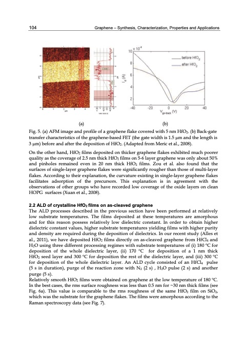
104 Graphene – Synthesis, Characterization, Properties and Applications (a) (b) Fig. 5. (a) AFM image and profile of a graphene flake covered with 5 nm HfO2. (b) Back-gate transfer characteristics of the graphene-based FET (the gate width is 1.5 m and the length is 3 m) before and after the deposition of HfO2. (Adapted from Meric et al., 2008). On the other hand, HfO2 films deposited on thicker graphene flakes exhibited much poorer quality as the coverage of 2.5 nm thick HfO2 films on 5-6 layer graphene was only about 50% and pinholes remained even in 20 nm thick HfO2 films. Zou et al. also found that the surfaces of single-layer graphene flakes were significantly rougher than those of multi-layer flakes. According to their explanation, the curvature existing in single-layer graphene flakes facilitates adsorption of the precursors. This explanation is in agreement with the observations of other groups who have recorded low coverage of the oxide layers on clean HOPG surfaces (Xuan et al., 2008). 2.2 ALD of crystalline HfO2 films on as-cleaved graphene The ALD processes described in the previous section have been performed at relatively low substrate temperatures. The films deposited at these temperatures are amorphous and for this reason possess relatively low dielectric constant. In order to obtain higher dielectric constant values, higher substrate temperatures yielding films with higher purity and density are required during the deposition of dielectrics. In our recent study (Alles et al., 2011), we have deposited HfO2 films directly on as-cleaved graphene from HfCl4 and H2O using three different processing regimes with substrate temperatures of (i) 180 oC for deposition of the whole dielectric layer, (ii) 170 oC for deposition of a 1 nm thick HfO2 seed layer and 300 oC for deposition the rest of the dielectric layer, and (iii) 300 oC for deposition of the whole dielectric layer. An ALD cycle consisted of an HfCl4 pulse (5 s in duration), purge of the reaction zone with N2 (2 s) , H2O pulse (2 s) and another purge (5 s). Relatively smooth HfO2 films were obtained on graphene at the low temperature of 180 oC. In the best cases, the rms surface roughness was less than 0.5 nm for ~30 nm thick films (see Fig. 6a). This value is comparable to the rms roughness of the same HfO2 film on SiO2, which was the substrate for the graphene flakes. The films were amorphous according to the Raman spectroscopy data (see Fig. 7).PDF Image | GRAPHENE SYNTHESIS CHARACTERIZATION PROPERTIES
PDF Search Title:
GRAPHENE SYNTHESIS CHARACTERIZATION PROPERTIESOriginal File Name Searched:
Graphene-Synthesis.pdfDIY PDF Search: Google It | Yahoo | Bing
Salgenx Redox Flow Battery Technology: Power up your energy storage game with Salgenx Salt Water Battery. With its advanced technology, the flow battery provides reliable, scalable, and sustainable energy storage for utility-scale projects. Upgrade to a Salgenx flow battery today and take control of your energy future.
| CONTACT TEL: 608-238-6001 Email: greg@infinityturbine.com | RSS | AMP |