PDF Publication Title:
Text from PDF Page: 003
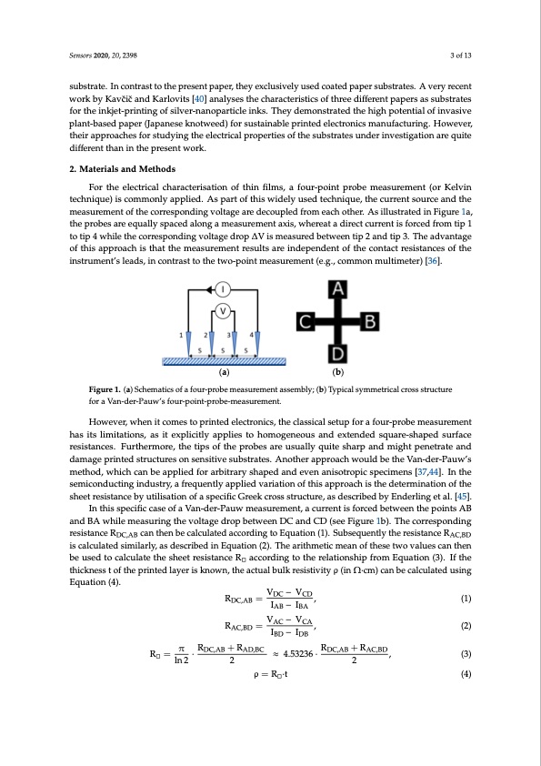
Sensors 2020, 20, 2398 3 of 13 substrate. In contrast to the present paper, they exclusively used coated paper substrates. A very recent Sensors 2020, 20, x 3 of 13 work by Kavcˇicˇ and Karlovits [40] analyses the characteristics of three different papers as substrates for the inkjet-printing of silver-nanoparticle inks. They demonstrated the high potential of invasive different papers as substrates for the inkjet-printing of silver-nanoparticle inks. They demonstrated plant-based paper (Japanese knotweed) for sustainable printed electronics manufacturing. However, the high potential of invasive plant-based paper (Japanese knotweed) for sustainable printed their approaches for studying the electrical properties of the substrates under investigation are quite electronics manufacturing. However, their approaches for studying the electrical properties of the dsuiffbesrternatetshuandinerthinevpersetsigeantiownoarkre. quite different than in the present work. 2. Materials and Methods 2. Materials and Methods For the electrical characterisation of thin films, a four-point probe measurement (or Kelvin For the electrical characterisation of thin films, a four-point probe measurement (or Kelvin technique) is commonly applied. As part of this widely used technique, the current source and the technique) is commonly applied. As part of this widely used technique, the current source and the measurement of the corresponding voltage are decoupled from each other. As illustrated in Figure 1a, measurement of the corresponding voltage are decoupled from each other. As illustrated in Figure the probes are equally spaced along a measurement axis, whereat a direct current is forced from tip 1 1a, the probes are equally spaced along a measurement axis, whereat a direct current is forced from to tip 4 while the corresponding voltage drop ∆V is measured between tip 2 and tip 3. The advantage tip 1 to tip 4 while the corresponding voltage drop ∆V is m2206easured between tip 2 and tip 3. The of this approach is that the measurement results are independent of the contact resistances of the advantage of this approach is that the measurement results are independent of the contact resistances instrument’s leads, in contrast to the two-point measurement (e.g., common multimeter) [36]. of the instrument’s leads, in contrast to the two-point measurement (e.g., common multimeter) [36]. (a) (b) Figure11..(a()aS)cShcehmeamtiactsicosfaofoaur-fpourorb-permobeeasumreamseunretmasesnemtbalsys;e(mbb)Tly;p(ibca)lTsympimcaeltrsicyamlcmroestsrisctarluctruorses fsotruacVtuarne-dfoer-aPVauawn-’dsefro-uPra-upwoi’nst-fpourorb-peo-mineta-psurorbeme-meneta. surement. However, when it comes to printed electronics, the classical setup for a four-probe measurement However, when it comes to printed electronics, the classical setup for a four-probe measurement has its limitations, as it explicitly applies to homogeneous and extended square-shaped surface has its limitations, as it explicitly applies to homogeneous and extended square-shaped surface resistances. Furthermore, the tips of the probes are usually quite sharp and might penetrate and resistances. Furthermore, the tips of the probes are usually quite sharp and might penetrate and damage printed structures on sensitive substrates. Another approach would be the Van-der-Pauw’s damage printed structures on sensitive substrates. Another approach would be the Van-der-Pauw’s method, which can be applied for arbitrary shaped and even anisotropic specimens [37,44]. In the method, which can be applied for arbitrary shaped and even anisotropic specimens [37,44]. In the semiconducting industry, a frequently applied variation of this approach is the determination of the semiconducting industry, a frequently applied variation of this approach is the determination of the sheet resistance by utilisation of a specific Greek cross structure, as described by Enderling et al. [45]. sheet resistance by utilisation of a specific Greek cross structure, as described by Enderling et al. [45]. In this specific case of a Van-der-Pauw measurement, a current is forced between the points AB In this specific case of a Van-der-Pauw measurement, a current is forced between the points AB and BA while measuring the voltage drop between DC and CD (see Figure 1b). The corresponding and BA while measuring the voltage drop between DC and CD (see Figure 1b). The corresponding resistanceR ,canthenbecalculatedaccordingtoEquation(1).SubsequentlytheresistanceR resistance RDC,AB can then be calculated according to Equation (1). Subsequently the resisAtaCn,BcDe R is calculated similarly, as described in Equation (2). The arithmetic mean of these two values can then , is calculated similarly, as described in Equation (2). The arithmetic mean of these two values can then be used to calculate the sheet resistance R thickness t of the printed layer is known, the actual bulk resistivity ρ (in Ω·cm) can be calculated using (1) (1) (2) (2) be used to calculate the sheet resistance R according to the relationship from Equation (3). If the □ If the thickness t of the printed layer is known, the actual bulk resistivity ρ (in Ω∙cm) can be Equation (4). calculated using Equation (4). VDC − VCD RDC,AB= V V, R = ln 2 · R AB BA, according to the relationship from Equation (3). , I − I I I RAC,BD = VAC − VCA , I V −I V π R, BD DB, RDC,AB + RAD,BC I I RDC,AB + RAC,BD 2 ≈ 4.53236 · R π ∙ R, R, 4.53236 ∙ R, R,, (3) , (3) □ ln2 2ρ=R·t 2 (4) ρ R□ ∙ t (4) The sheet resistance of inkjet-printed silver nanoparticle ink (Sicrys 115-TM119; particle size d50 = 85 nm, d90 = 120 nm; viscosity 34 cP [46]) on two different, uncoated, commercially available paper substrates after photonic curing (PulseForge 1200) is observed. One of the paper substrates has a 2PDF Image | Inkjet-Printed Ag-Layers on Flexible, Uncoated Paper Substrates
PDF Search Title:
Inkjet-Printed Ag-Layers on Flexible, Uncoated Paper SubstratesOriginal File Name Searched:
sensors-20-02398-v2.pdfDIY PDF Search: Google It | Yahoo | Bing
Turbine and System Plans CAD CAM: Special for this month, any plans are $10,000 for complete Cad/Cam blueprints. License is for one build. Try before you buy a production license. More Info
Waste Heat Power Technology: Organic Rankine Cycle uses waste heat to make electricity, shaft horsepower and cooling. More Info
All Turbine and System Products: Infinity Turbine ORD systems, turbine generator sets, build plans and more to use your waste heat from 30C to 100C. More Info
CO2 Phase Change Demonstrator: CO2 goes supercritical at 30 C. This is a experimental platform which you can use to demonstrate phase change with low heat. Includes integration area for small CO2 turbine, static generator, and more. This can also be used for a GTL Gas to Liquids experimental platform. More Info
Introducing the Infinity Turbine Products Infinity Turbine develops and builds systems for making power from waste heat. It also is working on innovative strategies for storing, making, and deploying energy. More Info
Need Strategy? Use our Consulting and analyst services Infinity Turbine LLC is pleased to announce its consulting and analyst services. We have worked in the renewable energy industry as a researcher, developing sales and markets, along with may inventions and innovations. More Info
Made in USA with Global Energy Millennial Web Engine These pages were made with the Global Energy Web PDF Engine using Filemaker (Claris) software.
Infinity Turbine Developing Spinning Disc Reactor SDR or Spinning Disc Reactors reduce processing time for liquid production of Silver Nanoparticles.
| CONTACT TEL: 608-238-6001 Email: greg@infinityturbine.com | RSS | AMP |