
PDF Publication Title:
Text from PDF Page: 180
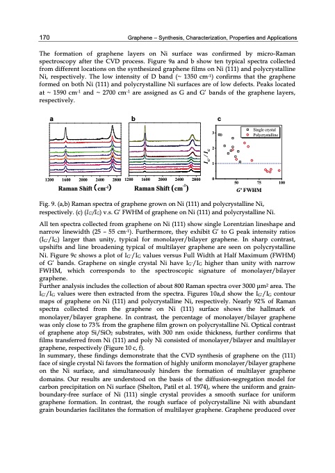
170 Graphene – Synthesis, Characterization, Properties and Applications The formation of graphene layers on Ni surface was confirmed by micro-Raman spectroscopy after the CVD process. Figure 9a and b show ten typical spectra collected from different locations on the synthesized graphene films on Ni (111) and polycrystalline Ni, respectively. The low intensity of D band (~ 1350 cm-1) confirms that the graphene formed on both Ni (111) and polycrystalline Ni surfaces are of low defects. Peaks located at ~ 1590 cm-1 and ~ 2700 cm-1 are assigned as G and G’ bands of the graphene layers, respectively. abc Single crystal Polycrystalline 1200 1600 2000 2400 2800 1200 1600 2000 2400 2800 0 50 75 100 Raman Shift ( cm-1) Raman Shift (cm-1) G' FWHM Fig. 9. (a,b) Raman spectra of graphene grown on Ni (111) and polycrystalline Ni, respectively. (c) (IG’/IG) v.s. G’ FWHM of graphene on Ni (111) and polycrystalline Ni. All ten spectra collected from graphene on Ni (111) show single Lorentzian lineshape and narrow linewidth (25 – 55 cm-1). Furthermore, they exhibit G’ to G peak intensity ratios (IG’/IG) larger than unity, typical for monolayer/bilayer graphene. In sharp contrast, upshifts and line broadening typical of multilayer graphene are seen on polycrystalline Ni. Figure 9c shows a plot of IG’/IG values versus Full Width at Half Maximum (FWHM) of G’ bands. Graphene on single crystal Ni have IG’/IG higher than unity with narrow FWHM, which corresponds to the spectroscopic signature of monolayer/bilayer graphene. Further analysis includes the collection of about 800 Raman spectra over 3000 μm2 area. The IG’/IG values were then extracted from the spectra. Figures 10a,d show the IG’/IG contour maps of graphene on Ni (111) and polycrystalline Ni, respectively. Nearly 92% of Raman spectra collected from the graphene on Ni (111) surface shows the hallmark of monolayer/bilayer graphene. In contrast, the percentage of monolayer/bilayer graphene was only close to 73% from the graphene film grown on polycrystalline Ni. Optical contrast of graphene atop Si/SiO2 substrates, with 300 nm oxide thickness, further confirms that films transferred from Ni (111) and poly Ni consisted of monolayer/bilayer and multilayer graphene, respectively (Figure 10 c, f). In summary, these findings demonstrate that the CVD synthesis of graphene on the (111) face of single crystal Ni favors the formation of highly uniform monolayer/bilayer graphene on the Ni surface, and simultaneously hinders the formation of multilayer graphene domains. Our results are understood on the basis of the diffusion-segregation model for carbon precipitation on Ni surface (Shelton, Patil et al. 1974), where the uniform and grain- boundary-free surface of Ni (111) single crystal provides a smooth surface for uniform graphene formation. In contrast, the rough surface of polycrystalline Ni with abundant grain boundaries facilitates the formation of multilayer graphene. Graphene produced over I/ G ' IG 3 2 1PDF Image | GRAPHENE SYNTHESIS CHARACTERIZATION PROPERTIES
PDF Search Title:
GRAPHENE SYNTHESIS CHARACTERIZATION PROPERTIESOriginal File Name Searched:
Graphene-Synthesis.pdfDIY PDF Search: Google It | Yahoo | Bing
Salgenx Redox Flow Battery Technology: Power up your energy storage game with Salgenx Salt Water Battery. With its advanced technology, the flow battery provides reliable, scalable, and sustainable energy storage for utility-scale projects. Upgrade to a Salgenx flow battery today and take control of your energy future.
| CONTACT TEL: 608-238-6001 Email: greg@infinityturbine.com | RSS | AMP |