
PDF Publication Title:
Text from PDF Page: 162
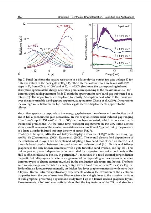
1252 Graphene – Synthesis, Characterization, Properties anWdill-bAe-psept-lbiyc-IaN-tTiEoCnHs Vb = –130 V 12 Experiment a) ) )%( D = 3.0 V nm –1 Ω 88 k ( ec ne ec re n fi V = 60 V b at d si n V b =0 V D = 1.9 V nm –1 se oit 44 R prosbA D = 1.4 V nm –1 D = 1.0 V nm –1 0 0 –10010 200400600 Vt (V) b) Energy (meV) 12 Fig. 7. Panel (a) shows the square resistance of a bilayer device versus top gate voltage Vt for different values of the back gate voltage Vb. The different colour traces are taken with 20V steps in Vb from 60V to −100V and at Vb = −130V. (b) shows the corresponding infrared absorption spectra at the charge neutrality point corresponding to the maximum of Rsq, for different applied displacement fields D (with the spectrum for zero band gap subtracted as a reference). The upper traces are displaced for clarity. Absorption peaks due to the transition over the gate tuneable band-gap are apparent, adapted from Zhang et al. (2009). D represents the average value between the top- and back-gate electric displacements applied to the bilayer. absorption spectra corresponds to the energy gap between the valence and conduction band and it has a pronounced gate tuneability. In this way an electric field induced gap ranging from 0 meV up to 250 meV at D = 3V/nm has been reported, which is consistent with theoretical predictions. At the same time, transport experiments in the very same devices show a small increase of the maximum resistance as a function of Eex confirming the presence of a large disorder induced sub-gap density of states, Fig. 7a. Contrary to bilayers, ABA-stacked trilayers display a decrease of Rmax with increasing E , sq ex see Fig. 8b (Craciun et al. (2009); Russo et al. (2009)). The overall electric field dependence of the resistance of trilayers can be explained adopting a two band model with an electric field tuneable band overlap between the conduction and valence band (δε). To this end trilayer graphene is the only known semimetal with a gate tuneable band overlap, see Fig. 8c . This unique property was independently demonstrated by magneto-transport experiments of the Hall coefficient (RH), see Fig. 8a. In particular, RH measured at a fixed external perpendicular magnetic field displays a characteristic sign reversal corresponding to the cross-over between different types of charge carriers involved in the conduction (electrons and holes). The back gate voltage range over which RH changes sign gives a band overlap δε ≈ 28 meV, see Fig. 8a. To date little is known experimentally on thicker few layer graphene materials with more than 3 layers. Recent infrared spectroscopy experiments address the evolution of the electronic properties from the one of mass-less Dirac electrons in a single layer to the massive particles of bulk graphite, presenting a systematic study from 1 up to 8 Bernal stacked graphene layers. Measurements of infrared conductivity show that the key features of the 2D band structurePDF Image | GRAPHENE SYNTHESIS CHARACTERIZATION PROPERTIES
PDF Search Title:
GRAPHENE SYNTHESIS CHARACTERIZATION PROPERTIESOriginal File Name Searched:
Graphene-Synthesis.pdfDIY PDF Search: Google It | Yahoo | Bing
Salgenx Redox Flow Battery Technology: Power up your energy storage game with Salgenx Salt Water Battery. With its advanced technology, the flow battery provides reliable, scalable, and sustainable energy storage for utility-scale projects. Upgrade to a Salgenx flow battery today and take control of your energy future.
| CONTACT TEL: 608-238-6001 Email: greg@infinityturbine.com | RSS | AMP |