PDF Publication Title:
Text from PDF Page: 128
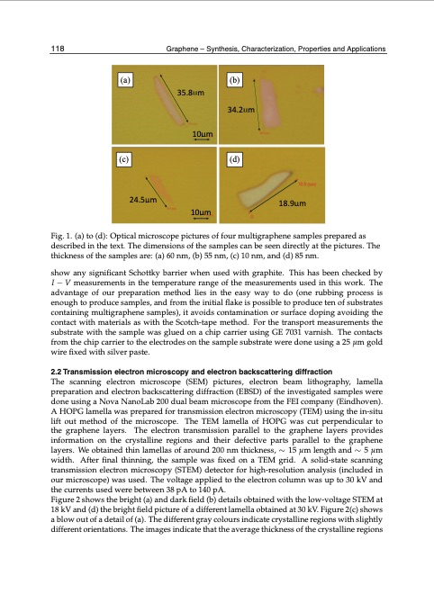
4118 (a) (c) 24.5μm Fig. 1. (a) to (d): Optical microscope pictures of four multigraphene samples prepared as described in the text. The dimensions of the samples can be seen directly at the pictures. The thickness of the samples are: (a) 60 nm, (b) 55 nm, (c) 10 nm, and (d) 85 nm. show any significant Schottky barrier when used with graphite. This has been checked by I − V measurements in the temperature range of the measurements used in this work. The advantage of our preparation method lies in the easy way to do (one rubbing process is enough to produce samples, and from the initial flake is possible to produce ten of substrates containing multigraphene samples), it avoids contamination or surface doping avoiding the contact with materials as with the Scotch-tape method. For the transport measurements the substrate with the sample was glued on a chip carrier using GE 7031 varnish. The contacts from the chip carrier to the electrodes on the sample substrate were done using a 25 μm gold wire fixed with silver paste. 2.2 Transmission electron microscopy and electron backscattering diffraction The scanning electron microscope (SEM) pictures, electron beam lithography, lamella preparation and electron backscattering diffraction (EBSD) of the investigated samples were done using a Nova NanoLab 200 dual beam microscope from the FEI company (Eindhoven). A HOPG lamella was prepared for transmission electron microscopy (TEM) using the in-situ lift out method of the microscope. The TEM lamella of HOPG was cut perpendicular to the graphene layers. The electron transmission parallel to the graphene layers provides information on the crystalline regions and their defective parts parallel to the graphene layers. We obtained thin lamellas of around 200 nm thickness, ∼ 15 μm length and ∼ 5 μm width. After final thinning, the sample was fixed on a TEM grid. A solid-state scanning transmission electron microscopy (STEM) detector for high-resolution analysis (included in our microscope) was used. The voltage applied to the electron column was up to 30 kV and the currents used were between 38 pA to 140 pA. Figure 2 shows the bright (a) and dark field (b) details obtained with the low-voltage STEM at 18 kV and (d) the bright field picture of a different lamella obtained at 30 kV. Figure 2(c) shows a blow out of a detail of (a). The different gray colours indicate crystalline regions with slightly different orientations. The images indicate that the average thickness of the crystalline regions Graphene – Synthesis, Characterization, Properties anWdill-bAe-psept-lbiyc-IaN-tTiEoCnHs (b) 35.8μm 34.2μm 10μm 10μm (d) 18.9μmPDF Image | GRAPHENE SYNTHESIS CHARACTERIZATION PROPERTIES
PDF Search Title:
GRAPHENE SYNTHESIS CHARACTERIZATION PROPERTIESOriginal File Name Searched:
Graphene-Synthesis.pdfDIY PDF Search: Google It | Yahoo | Bing
Salgenx Redox Flow Battery Technology: Power up your energy storage game with Salgenx Salt Water Battery. With its advanced technology, the flow battery provides reliable, scalable, and sustainable energy storage for utility-scale projects. Upgrade to a Salgenx flow battery today and take control of your energy future.
| CONTACT TEL: 608-238-6001 Email: greg@infinityturbine.com | RSS | AMP |