PDF Publication Title:
Text from PDF Page: 112
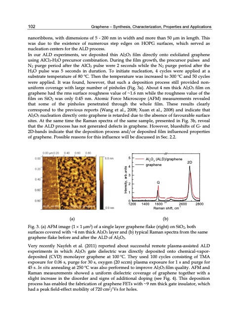
102 Graphene – Synthesis, Characterization, Properties and Applications nanoribbons, with dimensions of 5 - 200 nm in width and more than 50 m in length. This was due to the existence of numerous step edges on HOPG surfaces, which served as nucleation centers for the ALD process. In our ALD experiments, we deposited thin Al2O3 film directly onto exfoliated graphene using AlCl3-H2O precursor combination. During the film growth, the precursor pulses and N2 purge period after the AlCl3 pulse were 2 seconds while the N2 purge period after the H2O pulse was 5 seconds in duration. To initiate nucleation, 4 cycles were applied at a substrate temperature of 80 oC. Then the temperature was increased to 300 oC and 50 cycles were applied. It was found, however, that such a deposition process still provided non- uniform coverage with large number of pinholes (Fig. 3a). About 4 nm thick Al2O3 film on graphene had the rms surface roughness value of ~1.6 nm while the roughness value of the film on SiO2 was only 0.45 nm. Atomic Force Microscope (AFM) measurements revealed that some of the pinholes penetrated through the whole film. These results clearly correspond to the previous reports (Wang et al., 2008; Xuan et al., 2008) and indicate that Al2O3 nucleation directly onto graphene is retarded due to the absence of favourable surface sites. At the same time the Raman spectra of the same sample, presented in Fig. 3b, reveal that the ALD process has not generated defects in graphene. However, blueshifts of G- and 2D-bands indicate that the deposition process and/or deposited film influenced properties of graphene. Possible reasons for this influence will be discussed in Sec. 2.2. 5 Al2O3 (ALD)/graphene graphene 4 stinu.b 3 ra,yti G 2 snetnI 1 0 1200 1400 1600 2600 Raman shift, cm-1 (b) 2D 2800 (a) Fig. 3. (a) AFM image (1 1 m2) of a single layer graphene flake (right) on SiO2, both surfaces covered with ~4 nm thick Al2O3 layer and (b) typical Raman spectra from the same graphene flake before and after the ALD of Al2O3. Very recently Nayfeh et al. (2011) reported about successful remote plasma-assisted ALD experiments in which Al2O3 gate dielectric was directly deposited onto chemical-vapor- deposited (CVD) monolayer graphene at 100 oC. They used 100 cycles consisting of TMA exposure for 0.06 s, purge for 30 s, oxygen (20 sccm) plasma exposure for 1 s and purge for 45 s. In situ annealing at 250 oC was also performed to improve Al2O3 film quality. AFM and Raman measurements showed a uniform dielectric coverage of graphene together with a slight increase in the disorder and signs of additional doping (see Fig. 4). This deposition process has enabled the fabrication of graphene FETs with ~9 nm thick gate insulator, which had a peak field-effect mobility of 720 cm2/Vs for holes.PDF Image | GRAPHENE SYNTHESIS CHARACTERIZATION PROPERTIES
PDF Search Title:
GRAPHENE SYNTHESIS CHARACTERIZATION PROPERTIESOriginal File Name Searched:
Graphene-Synthesis.pdfDIY PDF Search: Google It | Yahoo | Bing
Salgenx Redox Flow Battery Technology: Power up your energy storage game with Salgenx Salt Water Battery. With its advanced technology, the flow battery provides reliable, scalable, and sustainable energy storage for utility-scale projects. Upgrade to a Salgenx flow battery today and take control of your energy future.
| CONTACT TEL: 608-238-6001 Email: greg@infinityturbine.com | RSS | AMP |