
PDF Publication Title:
Text from PDF Page: 183
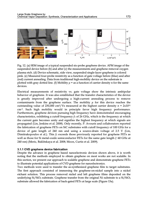
Large Scale Graphene by Chemical Vapor Deposition: Synthesis, Characterization and Applications 173 ef Fig. 12. (a) SEM image of a typical suspended six-probe graphene device. AFM image of the suspended device before (b) and after (c) the measurements and graphene removal oxygen plasma etch. (d) Device schematic, side view, suspended single-layer graphene is colored pink. (e) Measured four-probe resistivity as a function of gate voltage before (blue) and after (red) current annealing. Data from traditional high-mobility device on the substrate is plotted with gray dotted line. (f) Mobility μ = as a function of carrier density n for the same devices. Electrical measurements of resistivity vs. gate voltage show the intrinsic ambipolar behavior of graphene. It was also established that the transfer characteristics of the device is greatly improved after undergoing a high-current annealing process to remove contaminants from the graphene surface. The mobility μ for this device reaches the outstanding value of 230,000 cm2/Vs measured at the highest carrier density n = 2x1011 cm-2. Such high mobility would in principle favor high frequency performance. Furthermore, graphene devices pursuing high frequency have demonstrated encouraging characteristics, exhibiting a cutoff frequency fT of 26 GHz, which is the frequency at which the current gain becomes unity and signifies the highest frequency at which signals are propagated (Lin, Jenkins et al. 2008). Only recently, P. Avouris and collaborators reported the fabrication of graphene FETs on SiC substrates with cutoff frequency of 100 GHz for a device of gate length of 240 nm and using a source-drain voltage of 2.5 V (Lin, Dimitrakopoulos et al.). This fT exceeds those previously reported for graphene FETs as well as those for Si metal-oxide semiconductor FETs for the same gate length (~40 GHz at 240 nm) (Meric, Baklitskaya et al. 2008; Moon, Curtis et al. 2009). 3.1.1 CVD graphene device fabrication Despite the advance in graphene based nanoelectronic devices shown above, it is worth noting that the methods employed to obtain graphene on most works are not scalable. In this section, we present our approach to scalable graphene and demonstrate graphene FETs to illustrate potential applications of CVD graphene for nanoelectronics. Two methods were used to transfer the as-synthesized graphene film to target substrates. The first approach consisted of immersing the graphene-on-nickel sample into a nickel etchant solution. This process removed nickel and left graphene films deposited on the underlying Si/SiO2 substrate. Graphene transfer from the original Ni substrate to a Si/SiO2 substrate allowed the fabrication of back-gated FETs at large scale (Figure 13a).PDF Image | GRAPHENE SYNTHESIS CHARACTERIZATION PROPERTIES
PDF Search Title:
GRAPHENE SYNTHESIS CHARACTERIZATION PROPERTIESOriginal File Name Searched:
Graphene-Synthesis.pdfDIY PDF Search: Google It | Yahoo | Bing
Salgenx Redox Flow Battery Technology: Power up your energy storage game with Salgenx Salt Water Battery. With its advanced technology, the flow battery provides reliable, scalable, and sustainable energy storage for utility-scale projects. Upgrade to a Salgenx flow battery today and take control of your energy future.
| CONTACT TEL: 608-238-6001 Email: greg@infinityturbine.com | RSS | AMP |