
PDF Publication Title:
Text from PDF Page: 175
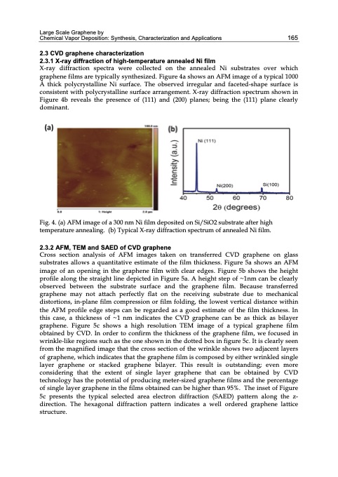
Large Scale Graphene by Chemical Vapor Deposition: Synthesis, Characterization and Applications 165 2.3 CVD graphene characterization 2.3.1 X-ray diffraction of high-temperature annealed Ni film X-ray diffraction spectra were collected on the annealed Ni substrates over which graphene films are typically synthesized. Figure 4a shows an AFM image of a typical 1000 Å thick polycrystalline Ni surface. The observed irregular and faceted-shape surface is consistent with polycrystalline surface arrangement. X-ray diffraction spectrum shown in Figure 4b reveals the presence of (111) and (200) planes; being the (111) plane clearly dominant. Fig. 4. (a) AFM image of a 300 nm Ni film deposited on Si/SiO2 substrate after high temperature annealing. (b) Typical X-ray diffraction spectrum of annealed Ni film. 2.3.2 AFM, TEM and SAED of CVD graphene Cross section analysis of AFM images taken on transferred CVD graphene on glass substrates allows a quantitative estimate of the film thickness. Figure 5a shows an AFM image of an opening in the graphene film with clear edges. Figure 5b shows the height profile along the straight line depicted in Figure 5a. A height step of ~1nm can be clearly observed between the substrate surface and the graphene film. Because transferred graphene may not attach perfectly flat on the receiving substrate due to mechanical distortions, in-plane film compression or film folding, the lowest vertical distance within the AFM profile edge steps can be regarded as a good estimate of the film thickness. In this case, a thickness of ~1 nm indicates the CVD graphene can be as thick as bilayer graphene. Figure 5c shows a high resolution TEM image of a typical graphene film obtained by CVD. In order to confirm the thickness of the graphene film, we focused in wrinkle-like regions such as the one shown in the dotted box in figure 5c. It is clearly seen from the magnified image that the cross section of the wrinkle shows two adjacent layers of graphene, which indicates that the graphene film is composed by either wrinkled single layer graphene or stacked graphene bilayer. This result is outstanding; even more considering that the extent of single layer graphene that can be obtained by CVD technology has the potential of producing meter-sized graphene films and the percentage of single layer graphene in the films obtained can be higher than 95%. The inset of Figure 5c presents the typical selected area electron diffraction (SAED) pattern along the z- direction. The hexagonal diffraction pattern indicates a well ordered graphene lattice structure.PDF Image | GRAPHENE SYNTHESIS CHARACTERIZATION PROPERTIES
PDF Search Title:
GRAPHENE SYNTHESIS CHARACTERIZATION PROPERTIESOriginal File Name Searched:
Graphene-Synthesis.pdfDIY PDF Search: Google It | Yahoo | Bing
Salgenx Redox Flow Battery Technology: Power up your energy storage game with Salgenx Salt Water Battery. With its advanced technology, the flow battery provides reliable, scalable, and sustainable energy storage for utility-scale projects. Upgrade to a Salgenx flow battery today and take control of your energy future.
| CONTACT TEL: 608-238-6001 Email: greg@infinityturbine.com | RSS | AMP |